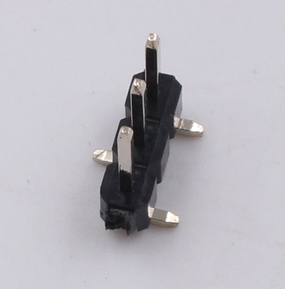
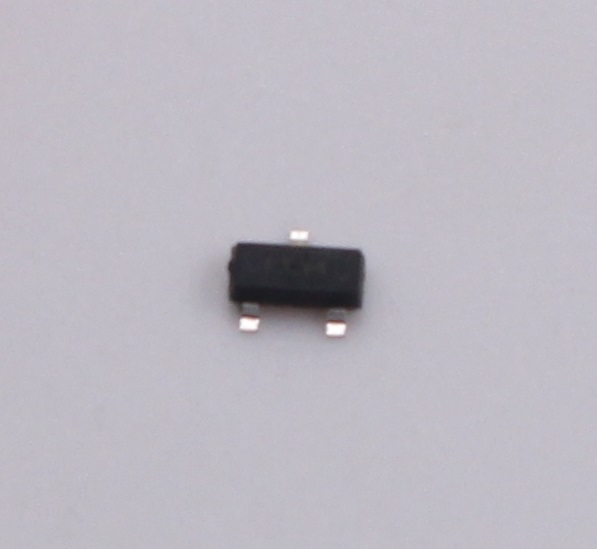
List of included components
Box 2 – Mechanical
Box 3 – Semiconductors
Box 4 – Resistors
Box 5 – Capacitors
| Reference | Marking | Value | Package | Description | Quantity | Picture |
|---|---|---|---|---|---|---|
| C1, C2, C3 | 10uF | 0805 | Decoupling capacitor | 3 |  | |
| C4, C5, C6, C7, C8 | 0.1uF | 0603 | Decoupling capacitor | 10 |  |
Box 6 – Soldering challenge
Reference designators
When drawing a circuit schematic each component is annotated with a unique reference designator. Most commonly they consist of a letter indicating the component type and succeeding digits incremented in sequence for each unique part starting from one. For example if the circuit has three resistors, they may be assigned designators R1, R2, and R3.
List of component types
| Letter | Component type |
|---|---|
| C | Capacitor |
| D | Diode |
| J | Jack (pin header or connector) |
| L | Inductor |
| Q | Transistor |
| R | Resistor |
| U | Integrated circuit |
| Y | Crystal or oscillator |
References
Unit of values
Units
| Symbol | Name | Description | Derivation |
|---|---|---|---|
| Ω / ohm | Ohm | resistance | 1 Ω = 1 V / 1 A |
| C | Coulomb | charge | 1 C = 1 A / 1 s |
| F | Farad | capacitance | 1 F = 1 C / 1 V |
| A | Ampere | current | 1 A = 1 C / s = 1 V / 1 Ω |
| J | Joule | energy | 1 J = 1 C * 1 V = 1 W × 1 s |
| V | Volt | voltage | 1 V = 1 J / C = 1 A × 1 Ω |
| W | Watt | power | 1 W = 1 J / s = 1 V × 1 A |
Unit prefixes
| Symbol | Name | Value (exponential) | Value (decimal) |
|---|---|---|---|
| p | pico | 10-12 | 0.000 000 000 001 |
| n | nano | 10-9 | 0.000 000 001 |
| µ / u | micro | 10-6 | 0.000 001 |
| m | milli | 10-3 | 0.001 |
| k | kilo | 103 | 1 000 |
| M | mega | 106 | 1 000 000 |
| G | giga | 109 | 1 000 000 000 |
References
- https://en.wikipedia.org/wiki/Ohm
- https://en.wikipedia.org/wiki/Coulomb
- https://en.wikipedia.org/wiki/Farad
- https://en.wikipedia.org/wiki/Ampere
- https://en.wikipedia.org/wiki/Joule
- https://en.wikipedia.org/wiki/Volt
- https://en.wikipedia.org/wiki/Watt
- https://en.wikipedia.org/wiki/Metric_prefix
Identifying resistor values
Three- and four-digit marking
R = m × 10n
The most common method for marking a 5% tolerance resistor value is using three digits representing an exponential number in scientific notation. Four digits can also be used. The first two or three digits are the mantissa (m) and the last digit is the exponent (n) with a base of 10.
Small values containing R
There’s a special case for small values where the letter R is added to notate the decimal point. Digits preceding the R represent the integer and the succeeding digits are the decimals.
Examples
A resistor marked 132 means the mantissa (two first digits) is 13. The exponent is the last digit which is 2. The resistor value would be 13 × 102 = 1300 or 1.3 kohm.
A resistor marked 1003 means the mantissa (three first digits) is 100. The exponent is the last digit which is 3. The resistor value would be 100 × 103 = 100 000 or 100 kohm.
A resistor marked 56R0 means the integer is 56. The decimals are 0. The resistor value would be 56.0 ohm.
A resistor marked R005 means the integer is 0. The decimals are 005. The resistor value would be 0.005 = 5 mohm.
References
Footprints
A footprint is the layout pattern on a circuit board for soldering a component. The simplest type consists of two square pads of exposed copper for soldering the component at both ends. The exposed copper is usually coated with soldering tin from the factory to prevent oxidation and easier soldering. This process is called HASL (hot air solder leveling). The DERULER project uses a different process called ENIG (electroless nickel immersion gold) that plates the copper with a nickel and gold layer to achieve the same result. In the past most components were of THT (hole-through technology) which relies on plated holes in the PCB for soldering. Today THT is usually only used for connectors and components that require improved mechanical support. Instead most components are now of SMD/SMT (surface-mount device/technology) type which is the only type used in this project.
Resistors and capacitors
Both chip resistors and capacitors (ceramic/MLCC/multi-layer chip capacitor) come in standardized sizes that are coded with their length and width in imperial units. There are metric equivalent codes but they’re not commonly used and has overlapping values which can be confusing. The component height can vary depending on the manufacturer and part number. Typically resistors are black and thin while capacitors are taller and brownish.
| Code (Imperial) | Size (L × W, imperial) | Code (metric) | Size (L × W, metric) |
|---|---|---|---|
| 0201 | 0.024 × 0.012 inch | 0603 | 0.6 × 0.3 mm |
| 0402 | 0.04 × 0.02 inch | 1005 | 1.0 × 0.5 mm |
| 0603 | 0.06 × 0.03 inch | 1608 | 1.55 × 0.85 mm |
| 0805 | 0.08 × 0.05 inch | 2012 | 2.0 × 1.2 mm |
| 1206 | 0.12 × 0.06 inch | 3216 | 3.2 × 1.6 mm |
| 2512 | 0.25 × 0.12 inch | 6332 | 6.3 × 3.2 mm |
Semiconductors
Many SMD semiconductors components follow standard footprints according to SO (small-outline) standards such as SOT (small-outline transistor), SOD (small-outline diode) or SOIC (small-outline integrated circuit) which are available in various sizes with different number of pins. Higher pin count ICs such as microcontrollers commonly use QFP (quad flat package) and more recently QFN (quad-flat no-leads package). In this project we’ve picked packages which are relatively simple to solder with a regular soldering iron and doesn’t require special tools such as a hot air soldering station.
References
- https://en.wikipedia.org/wiki/Hot_air_solder_leveling
- https://en.wikipedia.org/wiki/Electroless_nickel_immersion_gold
- https://en.wikipedia.org/wiki/Through-hole_technology
- https://en.wikipedia.org/wiki/Surface-mount_technology
- https://eepower.com/resistor-guide/resistor-standards-and-codes/resistor-sizes-and-packages/
- https://en.wikipedia.org/wiki/Small-outline_transistor
- https://en.wikipedia.org/wiki/Small_Outline_Diode
- https://en.wikipedia.org/wiki/Quad_flat_package
- https://en.wikipedia.org/wiki/Flat_no-leads_package


